 Jrok's Mappy to Dig Dug 2 Guide
|

Background
This is something I just put together fairly quickly, it should
all be accurate & I re-tested, from my original notes, on another Mappy to confirm it
still works. Let me know if there are any glaring omissions or errors.
To pre-empt anyone asking 'where are the ROMs ?'
Please visit somewhere such as.. http://www.romnation.net
Before you start
This conversion hack requires a certain level of technical ability so DO
NOT attempt this without the correct tools and some experience in board
level repair work.
Hardware
Mappy and Dig Dug 2 share very similar hardware, making conversion of a Mappy
boardset to run dig dug2 fairly straightforward. Both video and CPU pcb's
require some modification.
One significant part needed is a 56xx series custom IO controller
from a Super Pacman board, it is used to replace one of the 58xx IOC's on
Mappy.
Mappy uses two of the Namco 58xx I/O controllers, Dig dug 2 uses one 58xx and one 56xx. For reference superpac uses two 56xx.
Base Hardware Differences
| |
Program ROM |
Sprite ROM |
# of Sprites |
| Mappy |
24k ( 3 x 2764 ) |
16k ( 2 x 2764 ) |
128 |
| Dig Dug 2 |
32k ( 2 x 27128 ) |
32k ( 2 x 27128 ) |
256 |
The Real McCoy
To help protect the world against converted Mappy's being passed off as digdug 2's you can spot a 'bootleg' over an original in that
all the original DD2's I've seen, 3 so far, have a large 40pin custom IC on the video PCB near the video out molex connector.
Click for a picture of a real Dig Dug 2 video
PCB
Rom Names & locations
CPU Board
| ROM Name |
Size |
Location |
Type |
| DDUG2-1 BIN |
16,384 |
1B |
27128 EPROM |
| DDUG2-3 BIN |
16,384 |
1D |
27128 EPROM |
| DDUG2-4 BIN |
8192 |
1K |
2764 EPROM |
| |
|
|
|
| DDSND BIN |
256 |
3M |
82S126 PROM |
|
Video Board
| ROM Name |
Size |
Location |
Type |
| DDUG2-3B.BIN |
4096 |
3B |
2732 EPROM |
| DDUG2-3M.BIN |
16,384 |
3M |
27128 EPROM |
| DDUG2-3N.BIN |
16384 |
3N |
27128 EPROM |
| |
|
|
|
| DDCLR-4C.BIN |
256 |
4C |
82S126 PROM |
| DDCLR-5K.BIN |
256 |
5K |
82S126 PROM |
| DDCLR-5B.BIN |
32 |
5B |
82S123 PROM |
|
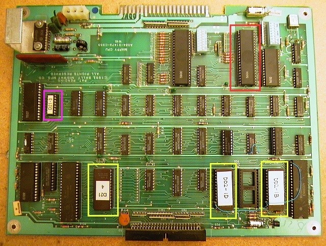
Board Modifications
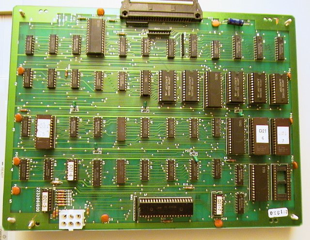
CPU Board
Dig dug 2 adds an extra 8k of program ROM, 32k using 2 x 16k EPROMs over Mappy's 24k, using 3 x 8K EPROMs.
The address decoder at 2C on the CPU board needs to be modified to allow
the new program roms to appear at $8000-bfff and $c000-ffff in the memory
map, A13 needs to be supplied to the two 27128 EPROMs A13 address lines, pin 26.
CPU board modifications
IC 2c, 74ls138 , pin 1 needs to be isolated from the PC
board ( Address line A13 )
pin 1 should be bent away from the PC board, to avoid contact and
jumpered to pin 16 of IC 2c.
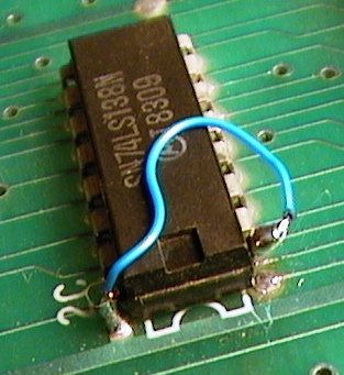
Two replacement Dig Dug 2 ROMs should be put into sockets 1B and
1D, with pin 26 bent out, so it's outside the socket.
These pins should be jumpered together and tied to A13, pin 21 of
the CPU 1A ( 6809 ).
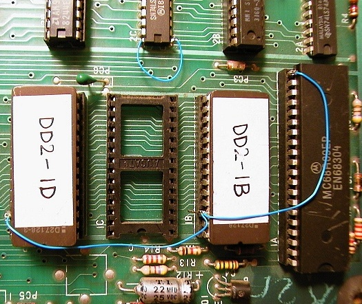
IO Controller, the 58xx at location 4C needs to be replaced with a 56xx from a super pacman board.
IOC at location 4F, 58xx, remains
the same.
|
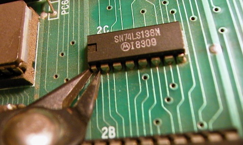
Step 1: Cutting pin 1 from the CPU board
|
|
Bend pin 1 away from PC board and solder a jumper
wire
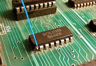
|
Jumper wire on Pin 1 tied to pin 16 ( +5v )
|
 |
ROM 1B & 1D pins 26 ( address line
A13) bent out from socket and jumpered together.
ROM A13 tied to pin 21 on 6809 CPU location 1A, cpu address
bus A13.
|
|
|
CPU board Layout
outlined areas areas are IC's to be replaced

|
|
|
| Video
Board
Dig dug 2 supports twice the number of sprites using two 27128 GFX roms,
mappy having only two 2764's. Adding the additional sprite support to a mappy involves piggy backing on an unused half of a 74LS74 on the video
PCB.
First some theory...
On the Mappy board location 4L - 74ls174 - controls sprite selection, it's uses a 5 bit value D2 - D6 for sprite number, low
bits 0,1 are passed directly to custom IC 12xx. This data comes from buffered address bus 3, which RAM 2N shares. /VSET clocks the data from the databus
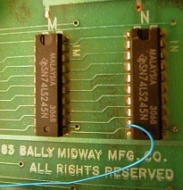
into 4L. The output 4L feeding the A12-A8 of the sprite ROMs 3L & 3N.
To add the support for the extra sprites you use the spare side of ic 2C,
74ls74, 'D' input is bit 7 of the buffered data bus 3, clk is /VSET and output 1Q controls the A13, pin 26, of two 27128's in location 3N and 3M, these replace the two 2764's.
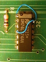
ic 2C pins 1, 4 and 13 all jumpered together |
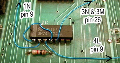
pin 1 & 4 are connected pin 13
pin 2 connected to D7 - pin 9 IC 1N - 74LS245
pin 3 connected to /VSET - pin 9 of 4L - 74LS174
pin 5 connected to A13 - pin 26 IC 3N and 3M
|
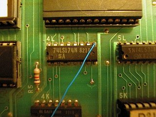
4L pin 9 jumpered to pin 3 ic 2C |
|
|
1N pin 9 jumpered to pin 2 ic 2C
|
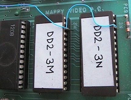
3M & 3N pins 26 bent out of socket and
connected together, also jumpered to pin 5 ic 2C
|
|
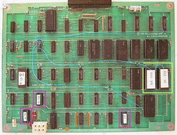
Video Board Layout
outlined areas areas are IC's to be replaced

|
|
Enhancements
In no particular order or timeframe...
- Modify the original code to use the 58xx IOC instead of requiring
the 56xx .
- High-score save upgrade
- Take a few more pictures
Back to JrokLand