Background
The Midway versions of Super Pacman and Mappy both use two PAL10L8's on the
CPU board, in the schematics they're labelled as SPC-5 and SPC-6. These are
effectively interchangable with the Namco SP1-2 and SP1-1 which appears on
Motos, Grobda, Phozon and Digdug 2, also the Namco version of the Super PacMan
board, uses the SP1-1 and SP1-2 while the mode common Midway version has the
SPC-5 and SPC-6 chips.
So just to be clear:
SP1-1 == SPC-6
SP1-2 == SPC-5
Observations
The two chips acts as address decoders for the primary and secondary CPU with some logic to control bus CPU bus access.
The SP1-1 is identical to the SPC-6
The SP1-2 is has one output equation different from the SPC-5, and also has a bug or two.
The SPC-5 and SP1-2 and a couple of bugs
From the Super Pacman schematics, and Mappy, the secondary CPU hardware
appears to support two EPROMs, a 2764 (8k EPROM) and a second
2732 (4k EPROM), this is controlled the ROMCS_32 in the equations, the ROMOE_32
output.
Also pin 21 of the 2732
( A11 ) is controlled through the SPC-5 & SP1-2 output pin 13, called
ROM_32_A11 in the
equations. In the schematics pin 21 is called "R/W" which isn't
correct for a 2732, but is for a 2k x 8 SRAM ( like a 6116 ), more on that
later.
The use of this extra ROM does not appear to have been
implemented in any actual games and probably for good reason, mostly because it
doesn't work using the SP1-2 logic.
A few interesting things here can be noted:
2732 ROM Addressing
SP1-2
ROMCS_32 decodes the EPROM chip enable at "001x XXXX XXXX XXXX" ( $2000-$3FFF
) in the
memory map.
ROMOE_32, is the 2732 output enable (/OE), is active low at address 110x
XXXX XXXX XXXX ($C000-DFFF ). This means the EPROM output enable would never
be active when the ROM is being addressed !
That looks like a bit of a bug in
the logic there.
SPC-5
ROMCS_32 decodes the EPROM chip enable at "110x XXXX XXXX XXXX" (
$C000-$DFFF )in the
memory map.
ROMOE, is the 2732 output enable ( /OE) and matches the ROMCS_32 decoding
with the addition that the 6809 R/W line needs to be logic high, so in a 6809
Read operation. So they fixed the SP1-2 4k EPROM chip enable bug with the SPC-5
However.... there's also an issue with the ROM_32_A11 ( aka. R/W ) output.
RAM Addressing & A11
Going back to the Super pacman schematics IC 1J listed as
a 2732 shows pin 21,
address line A11, of a 4k 2732 EPROM, connected pin 13 of the SPC-5, it's called
R/W in the schematic but I called it ROM_32_A11 in the equations.
A few definitions first:
1H* is a slowed 1H clock, so it's about 70ns behind the 1H clock, and transitions about 45ns after a transition of subE. See IC 2A on the super pacman schematics for how it's generated. 1H is 2x the frequency of the subE clock.
subE is the E clock for the sub-CPU, it's actually the 'Q' clock from the primary CPU, it's high for about 325ns.
ROM_32_A11 is active low on condition address lines SA15='1' & SA14 = '1' & SA13 = 0' ($Cxxx-DFFF) and subE ='1' and 1H* = '1'
Because of 1H* the output will be active low for about 1/2 the
subE cycle, but offset by 70ns.
Meaning the output will be active for only about 160ns. That's a bit
questionable for the address line on a slow (300ns) 2732 EPROM, but it would be
fine for the write strobe of an 150ns SRAM.
So ROM_32_A11 appears to be a designed for a write strobe for
an SRAM.
For A11 on an EPROM, if it was fast enough, it would
mean A11 would go inactive high while the 6809 completed the read cycle, so
there no way the lower half of the EPROM could be
selected, so effectively only 2K of the EPROM can be addressed as A11 would
always be high. It's only stable for about 110ns before the end of the 6809 read
cycle.
The problem here is that R/W is not taken into consideration in the logic so ANY
access from the 6809 either a read or write, to the address range $C000-DFFF would pull /CE
active and trigger the /WE write pulse turning even a read into a write ?!?
This is not ideal, it looks like a second bug in the
logic.
It could be corrected by an additional confition of "!RW" for the ROM_32_A11 equation which would cause /WE to be high (disabled) during a read operation, but still strobe during a write. Also in the case of an EPROM address A11 would be constantly high during the read cycle, so at least you'd get 2K of usable EPROM.
As no games seem to have used used extra ROM or RAM in this location the flaws don't really effect anything. On the boards the 28pin socket for the 2764 has pins 26,27,28 all pulled to +5v which means a 2732 could be dropped into the socket and work fine as a 4k EPROM. This is the case in Super Pacman. One of the Namco board variants has a 28pin socket with 24pin 2732 installed.
SPC-5 in Super Pac schematics
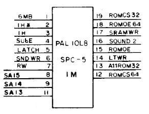
SPC-5 or SP1-2 Equations |
| // Note: 1H* is named H1s // pins 12, 13, 15,18,19 are not named in the schematic and are assigned names
// Note: -- SP1-2 equation differs // maps to $E000-$FFFF in memory map
// allows pass through writes of LATCH
writes from primary CPU
|
SPC-6 in Super Pac schematics
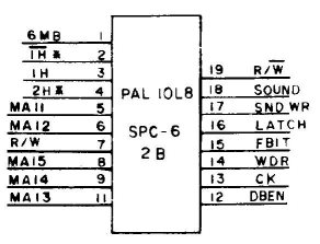
SPC-6 or SP1-1 Equations |
| // Note: // /1H* is named notH1s // 2H* is named H2s // R/W on the output is renamed RWq // unnamed pin 12 is named DBEN DBEN = H2s # MA15;
|